Basics of VLSI Design 7
Free Version
Publisher Description
Basics of VLSI Design - Complete Free handbook of VLSI with diagrams and graphs
The app is a complete free handbook of VLSI with diagrams and graphs. It is part of electronics & communications engineering education which brings important topics, notes, news & blog on the subject. Download the App as quick reference guide & ebook on this electronics & communications engineering subject.
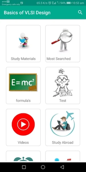
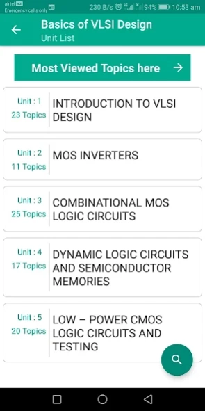
The app covers more than 90 topics of VLSI Design in detail. These topics are divided in 5 units.
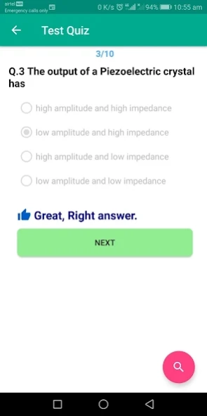
You can very easily pass and succeed in your exams or interviews, the app provides quick revision and reference to the topics like a detailed flash card.
Each topic is complete with diagrams, equations and other forms of graphical representations for easy understanding. Some of topics Covered in this application are:
1. Semiconductor memories :Introduction and types
2. Read Only Memory (ROM)
3. Three transistor DRAM cell
4. One transistor DRAM Cell
5. Flash memory
6. Low - Power CMOS Logic Circuits: Introduction
7. Design of CMOS inverters
8. MOS Inverters : introduction to switching characteristics
9. Scan-Based Techniques
10. Built-In Self Test (BIST) Techniques
11. Historical prospective of VLSI Design : Moore's Law
12. Classification of CMOS digital circuit types
13. A Circuit Design Example
14. VLSI Design methodologies
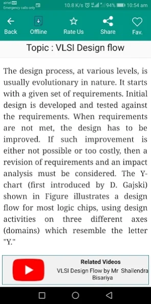
15. VLSI Design flow
16. Design Hierarchy
17. Concept of regularity, modularity and locality
18. CMOS fabrication
19. Fabrication Process Flow : Basic Steps
20. Fabrication of the nMOS transistor
21. CMOS fabrication : p-well process
22. CMOS fabrication : n-well process
23. CMOS fabrication : twin tub process
24. Stick diagrams and mask layout design
25. MOS transistor : physical structure
26. The MOS System under External Bias
27. Structure and operation of MOSFET
28. The threshold voltage
29. Current voltage characteristics of MOSFET
30. Mosfet scaling
31. Effects of scaling
32. Small Geometry Effects
33. MOS Capacitances
34. MOS inverter
35. Voltage transfer characteristics (VTC) of MOS inverter
36. Inverters with n-type MOSFET load
37. Resistive load inverter
38. Design of Depletion-Load Inverters
39. CMOS inverter
40. Delay time definitions
41. Calculation of Delay Times
42. Inverter Design with Delay Constrains : Example
43. Combinational MOS Logic Circuits : introduction
44. MOS Logic Circuits with Depletion nMOS Loads : Two-Input NOR Gate
45. MOS Logic Circuits with Depletion nMOS Loads : Generalized NOR structure with multiple inputs
46. MOS Logic Circuits with Depletion nMOS Loads : Transient analysis of NOR gate
47. MOS Logic Circuits with Depletion nMOS Loads : Two-Input NAND Gate
48. MOS Logic Circuits with Depletion nMOS Loads : Generalized NAND structure with multiple inputs
49. MOS Logic Circuits with Depletion nMOS Loads : Transient analysis of NAND gate
50. CMOS logic circuits : NOR2 (two input NOR ) gate
51. CMOS NAND2 (two input NAND) gate
52. Layout of Simple CMOS Logic Gates
53. Complex Logic Circuits
54. Complex CMOS Logic Gates
55. Layout of Complex CMOS Logic Gates
56. AOI and OAI Gates
57. Pseudo-nMOS Gates
58. CMOS Full-Adder Circuit & carry ripple adder
59. CMOS Transmission Gates (Pass Gates)
60. Complementary Pass-Transistor Logic (CPL)
61. Sequential MOS logic Circuits : Introduction
62. Behavior of Bistable Elements
63. The SR Latch Circuit
64. Clocked SR Latch
65. Clocked JK Latch
66. Master-Slave Flip-Flop
67. CMOS D-Latch and Edge-Triggered Flip-Flop
68. Dynamic Logic Circuits : Introduction
69. Basic Principles of Pass Transistor Circuits
All topics are not listed because of character limitations set by the Play Store.
About Basics of VLSI Design
Basics of VLSI Design is a free app for Android published in the Teaching & Training Tools list of apps, part of Education.
The company that develops Basics of VLSI Design is Engineering Apps. The latest version released by its developer is 7. This app was rated by 12 users of our site and has an average rating of 3.5.
To install Basics of VLSI Design on your Android device, just click the green Continue To App button above to start the installation process. The app is listed on our website since 2021-03-24 and was downloaded 374 times. We have already checked if the download link is safe, however for your own protection we recommend that you scan the downloaded app with your antivirus. Your antivirus may detect the Basics of VLSI Design as malware as malware if the download link to com.faadooengineers.free_vlsidesign is broken.
How to install Basics of VLSI Design on your Android device:
- Click on the Continue To App button on our website. This will redirect you to Google Play.
- Once the Basics of VLSI Design is shown in the Google Play listing of your Android device, you can start its download and installation. Tap on the Install button located below the search bar and to the right of the app icon.
- A pop-up window with the permissions required by Basics of VLSI Design will be shown. Click on Accept to continue the process.
- Basics of VLSI Design will be downloaded onto your device, displaying a progress. Once the download completes, the installation will start and you'll get a notification after the installation is finished.
